As part of ongoing face-to-face engagement between the F450C and G450C, members of both consortia gathered recently at M+W Group’s headquarters at the State University of New York Polytechnic Institute’s College of Nanoscale Science & Engineering (CNSE), nestled in the emerging technology hub in upstate New York, to discuss the status of facilities infrastructure projects supporting the semiconductor industry’s eventual transition to the 450mm wafer size.
Representatives of both organizations presented status updates on ongoing collaboration projects currently underway within the member companies. They also used the time to seek potential partners for scalable technology R&D efforts that can be used in both 300mm and 450mm high-volume manufacturing (HVM) environments.
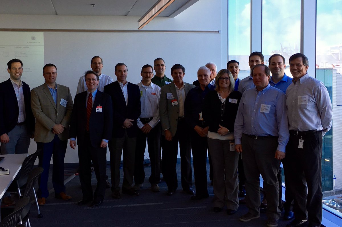
F450C and G450C members in attendance for the May 16 meeting at SUNY Poly’s Albany Site
David Skilbred, director of program coordination/management, G450C, kicked off the day by updating attendees on New York state’s efforts to support the activities of companies involved in the G450C wafer size transition.
Next, members were briefed about Haws Corporation’s transition to a new entity, Peek Process Insights Inc., led by Ben Peek. The new company is based in Portland, Oregon, and focuses on delivering an innovative data collection technology for advanced manufacturing processes.
Gary Hamilton, a F450C member company representative from CS CLEAN SYSTEMS, updated the group on the company’s innovative abatement systems that offer fabs low cost of ownership and the high efficiencies required in current and future HVM environments.
Next, Norm Fish, G450C process development engineer, spoke about current gas abatement technology challenges and reiterated G450C’s desire to collaborate with suppliers on R&D projects and provide support as needed to F450C members.
John DeGenova of Ovivo talked about the future water technology demands in advanced semiconductor manufacturing fabs, and focused on the need for water consumption efficiency in the 450mm environment. He noted that proven technologies exist to recover and reuse water in semiconductor facilities, and said that water economics will eventually drive the industry to integrate these technologies into future fabs.
The meeting closed with a status update on all active projects currently in progress. The attendees were updated on 450mm tool and equipment installs at CNSE’s NanoTech Complex, a 1.3 million square foot development “sandbox” featuring the industry’s only fully integrated 300mm and 450mm wafer pilot lines in 135,000 square feet of Class 1 capable cleanrooms.
F450C and G450C members will next meet at SEMICON West. Follow the F450C blog for updates.
Author: Todd Fosler
Program Manager – F450C
Project Development Director – M+W Group